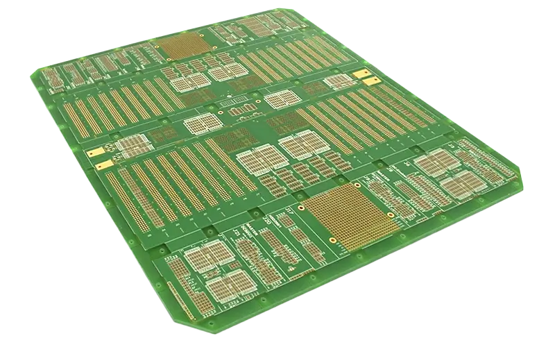
Multilayer PCBs
Today, electronic circuits connect so many components that there is no longer enough space for the conductors on the outer layers of a circuit board. Cables are therefore laid on inner copper layers. Vias provide the electrical connection between the inner and outer layers.
Multilayers are multi-talented
Multilayers are printed circuit boards with more than two layers of conductor tracks. Inner layers are used for routing the signals. Other inner layers are large-area power supply layers and serve as shielding layers for EMC-compliant design and HF PCBs.
Multilayers with 4, 6 and 8 layers are the most common. Backplanes with many connections and impedance-controlled PCBs with reference layers between the signal layers often require 10 or more layers, in rare cases 40 or more layers.
The most common copper thickness is 18 micrometers. Higher copper cross-sections of up to 400 micrometers are available for multilayers in power electronics.
Materials, technologies and tolerances
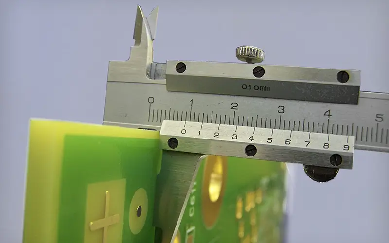
Maximum dimensions
mm
Up to
40
layers
Up to
12
mm thickness
12–400
µm
Aspect ratio up to
12:1
Minimum drill diameter
0.1
mm
Constructions
- Microvias
- Buried Vias
- Via Fill
- Thick copper
- All surfaces
- Solder resist
- Lettering
- Assembly benefits
For a complete list of our flex PCB fabrication capabilities, please refer to our capabilities section:
Some references
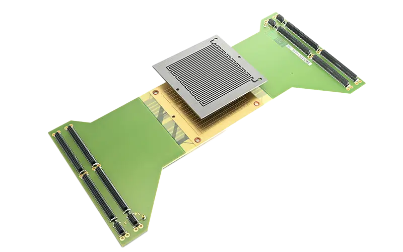
Test adapter for wafer probes
High-layer multilayer with 9 mm thickness as probe card for the construction of needle adapters in wafer probing, chip production and semiconductor testing.
Option 1: High-frequency material for testing RF and photonic chips.
Option 2: High-temperature material for semiconductor tests at higher temperatures.
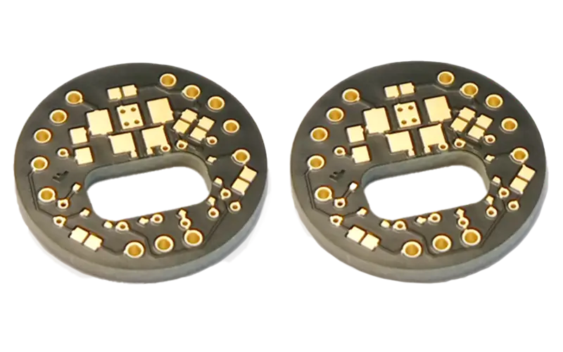
Sensors for hydrogen technology
The measurement of temperature and current density in fuel cells, electrolyzers and batteries enables the spatially resolved monitoring of electrochemical processes. Temperature and current sensors were integrated into the multilayer PCB for this purpose.
The technology is widely used in automotive development. Industrial energy technology, on the other hand, is aimed at use in series production.
Counterfeit protection
Multilayer with hidden identification features. This makes it possible to distinguish between original and plagiarism. The features are invisible for reverse engineering, but can be read directly by electrical means. This allows you to be informed by software if your assembly is counterfeit. External identification is no longer necessary.
Production guidelines for multilayer printed circuit boards
We manufactures all printed circuit boards according to the guidelines IPC-A-6012/6013 as standard in the following classes:
Class II is for general industrial production, i.e. appliances that are subject to higher demands and require high performance and a long service life.
Electronics in which continuous, uninterrupted operation is of crucial importance, for example in life-sustaining medical technology, in aircraft electronics such as flight controls and in safety-relevant applications.
Documentation and traceability of the entire production chain
We carry out the following tests:
- Electrical test according to IPC-9252
- Impedance control (TDR measurement method)
- Resistance measurement
- Milliohm measurement: four-wire method
- High-voltage test up to 500V
- EMPB (initial sample test report) with dimensions
- Layer thickness measurement (X-Ray)
- Micrograph analysis after solder shock test
- Solderability
- Preparation of CoC (Certificate of Conformity)
- Customer-specific tests by arrangement
- Application-specific tests by arrangement
Let us advise you free of charge!
We will be happy to help you:

Dr. Christoph Lehnberger
Head of Technology

Patrick Peek
Head of Sales
Frequently asked questions about multilayer PCBs
What is the difference between multilayer PCBs and simple PCBs?
Multilayer printed circuit boards consist of several layers of conductive material separated by insulation layers, which enables greater complexity and better performance, especially for applications with high packing density or requirements for signal stability and quality (signal integrity).
What materials are used for multilayers?
The most common base material is FR4, i.e. glass fiber-reinforced epoxy resin. Material manufacturers use this to produce so-called laminates or cores, i.e. copper-clad FR4. Flexible films for flex and rigid-flex printed circuit boards, material with low power loss for high-frequency applications and high-temperature material are also available.
What types of vias are used in multilayer printed circuit boards?
Vias are plated-through holes through all layers that connect the individual layers with each other. There are also blind vias (blind holes) or, in the case of small diameters, microvias, which are usually only drilled from the outside onto the next layer. Buried vias (buried holes) connect inner layers without reaching onto the outer layers. Filled & capped vias (plugged holes) are filled with resin and metallized after copper plating. Vias and buried vias can be filled in this way. Finally, vias can be partially drilled away during backdrilling for HF reasons.
Why is impedance control important?
High-frequency signals require the correct ratio of inductive and capacitive coupling to the surrounding reference potential. If the impedances are not consistently correct, the signals are reflected at the interference points. In the worst-case scenario, an HF signal will not reach the end of the line even though the path for direct current is clear.
How can thermal management in multilayer PCBs be optimized?
There is a patent recipe for dissipating heat from electronic assemblies: “area” in the sense of “cross-section”. To avoid thermal bottlenecks, heat paths with sufficient heat conduction over a sufficient cross-section must be planned. You can find out more about this under Power PCBs.
